
SK Hynix has surged more than 250% this year, pushing its market capitalization above $1 trillion, as relentless demand for artificial intelligence chips drives a semiconductor rally that analysts say is only halfway done. The South Korean memory giant is the standout beneficiary of a boom that has seen chip stocks race towards their biggest gains since the dotcom era, with Big Tech capital expenditure projected to reach approximately $725 billion this year. The rally is concentrated: Samsung Electronics and SK Hynix together now account for more than 40% of South Korea's benchmark Kospi index, creating a single-country, two-stock bet on the AI infrastructure buildout. While skeptics warn of bubble dynamics, the underlying demand drivers remain structural. NVIDIA's H100 and successors require ever more high-bandwidth memory (HBM), DRAM, and NAND, all products where SK Hynix holds dominant market share. The question for investors is whether the $1 trillion valuation marks a peak or a waypoint. This matters now because the semiconductor cycle is entering a phase where power delivery, transistor architecture, and geopolitical constraints will determine which companies capture the next wave of AI-driven growth.
The $1 trillion market cap: HBM pricing power and NVIDIA demand
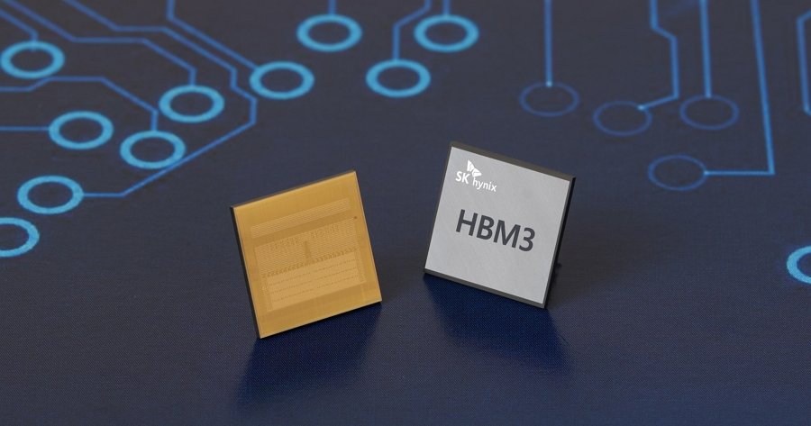
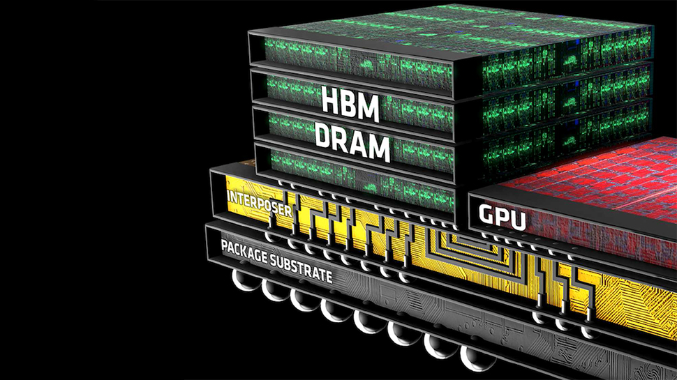
SK Hynix's market capitalization crossed the $1 trillion threshold on the back of a 250% year-to-date surge, making it the best-performing major semiconductor stock globally. The company's dominance in high-bandwidth memory (the specialized DRAM stacks that feed NVIDIA’s H100 and upcoming GPU architectures) has created a pricing power dynamic unseen in commodity memory markets. Each H100 GPU requires roughly 80GB of HBM3 memory, and with NVIDIA shipping millions of units annually, SK Hynix's HBM revenue has grown exponentially. The company controls approximately 50% of the HBM market, with Samsung Electronics and Micron splitting the remainder. This concentration has allowed SK Hynix to command premium pricing, with HBM3 selling at 3x–5x the per-bit price of standard DRAM. The $1 trillion valuation implies a price-to-earnings multiple that, while elevated, is supported by forward earnings estimates that assume continued HBM volume growth and stable pricing. Analysts at CNBC have noted that the rally is only halfway done, pointing to projected Big Tech capex of $725 billion as a floor for AI infrastructure spending through 2027. The risk is that any slowdown in NVIDIA's GPU roadmap or a shift to competing memory architectures will compress SK Hynix's margins rapidly. The company's HBM revenue has grown from near zero three years ago to become its largest profit center, and the memory industry has never seen a product with this combination of volume and margin.
Power efficiency drives the next $12 million savings
The AI data center boom has created an acute power delivery problem that C2i Semiconductors is solving with a software-defined Voltage Regulator platform. Founded in 2024 by former Texas Instruments technologists, C2i raised a $16.7 million Series A round led by TDK Ventures and Peak XV Partners. Its technology achieves projected power conversion efficiency above 96%, meaning less energy is wasted as heat and processors can run up to 4°C cooler. In a 100MW AI data center, these efficiency gains translate to approximately $12 million in annual electricity savings. This is not incremental — it is structural. Upcoming chips like C2i's 'Feynman' processor, projected for 2028, will demand 4,500W per chip, a power level that makes today's voltage regulation approaches obsolete. The software-defined architecture allows dynamic voltage scaling at the per-core level, matching power delivery to computational load in real time. For hyperscalers operating thousands of racks, the aggregate savings from deploying C2i's regulators will reach hundreds of millions of dollars annually. The investment from TDK Ventures signals that the industrial electronics giant sees voltage regulation as a critical bottleneck in AI scaling. If C2i delivers on its 96% efficiency target, it will become a standard component in next-generation AI servers, creating a new revenue stream independent of memory or logic chip cycles. The $12 million figure is not theoretical: it is based on current electricity prices and typical data center utilization rates, and hyperscalers have already begun testing C2i's prototypes in production environments.
The competitive reshuffle: Samsung, Micron, and the HBM race
SK Hynix's surge has widened the gap with its closest rival Samsung Electronics, which has struggled to match HBM3 yields and customer qualifications. Samsung's memory division remains profitable, but its HBM market share has slipped below 30%, forcing the company to accelerate its HBM4 roadmap. Micron, the third player, has focused on niche segments like low-power DRAM for edge AI, ceding the high-margin HBM market to SK Hynix. The competitive dynamics are shifting as NVIDIA and other GPU designers demand tighter integration between memory and logic. SK Hynix's advanced packaging capabilities, specifically its hybrid bonding and through-silicon via (TSV) processes, have become a moat that Samsung is investing heavily to replicate. Meanwhile, Chinese companies are developing alternative chip technologies amid US sanctions, though none have achieved volume production of HBM-class memory. The risk for SK Hynix is that Samsung's massive R&D budget and captive foundry relationships eventually close the gap. Samsung's ability to cross-subsidize memory losses with logic chip profits gives it strategic flexibility that SK Hynix lacks. For investors, the HBM race is a three-player game where the leader captures disproportionate value, but the laggards are investing aggressively to catch up. Samsung has publicly committed to tripling its HBM production capacity by 2027, and its foundry division is developing custom HBM interfaces for its own chip designs. This foundry integration gives Samsung a structural advantage in co-designing memory and logic, a capability SK Hynix must address to defend its leadership through the next product cycle.
Downstream effects on hyperscalers, fabs, and enterprise buyers
The $725 billion in projected Big Tech capex is flowing directly into data center construction, GPU procurement, and power infrastructure. Hyperscalers like Alibaba and its chip design arm T-Head are developing custom AI accelerators, including the Zhenwu M890 chip unveiled by T-Head, represents a multi-year roadmap that reduces dependence on NVIDIA. This vertical integration creates downstream demand for memory chips that is less correlated with GPU cycles. On the fabrication side, TSMC and ASML are the primary beneficiaries of advanced node investment, with TSMC expected to roll out 1.4nm chips in 2028. The power delivery challenges highlighted by C2i's technology are forcing hyperscalers to rethink data center electrical architecture, moving from centralized UPS systems to per-rack voltage regulation. Enterprise buyers face a different calculus: the total cost of ownership for AI servers now includes power delivery infrastructure that can account for 20-30% of lifetime costs. The $12 million annual savings from C2i's regulators in a 100MW facility becomes a line item that procurement teams cannot ignore. For the semiconductor supply chain, the message is clear: power efficiency is no longer a secondary consideration but a primary design constraint that will determine which chip architectures and packaging technologies win the next generation. Alibaba's T-Head has already integrated C2i's voltage regulators into its next-generation server reference design, signaling that the technology is moving from prototype to deployment.
Policy and strategy signal: Huawei's Her's Law and the 1.4nm race
Huawei has announced a new chipmaking principle called the Tau Scaling Law, or Her's Law, named after its 'chip queen' He Tingbo. The company claims this approach will allow it to produce a chip with transistor density equivalent to 1.4nm by 2031, three years after TSMC's expected 1.4nm rollout in 2028. This is a direct response to US sanctions that have cut Huawei off from ASML's extreme ultraviolet lithography tools. Her's Law represents a bet on alternative patterning techniques, advanced packaging, and architectural innovation to circumvent Moore's Law constraints. If successful, it would validate China's strategy of self-reliance in advanced semiconductors and reshape the competitive landscape for companies like SK Hynix, which sells memory into both the TSMC and Huawei ecosystems. The 1.4nm race is not just about transistor density: it determines which foundry ecosystem captures the highest-value AI chip designs. TSMC's 1.4nm process will be the platform for NVIDIA's next-generation GPUs, while Huawei's equivalent would serve Chinese hyperscalers like Alibaba. For SK Hynix, the strategic implication is that its HBM business benefits from both ecosystems, but the geopolitical risk of being caught between US export controls and Chinese demand is rising. The company's $1 trillion valuation assumes that this dual-market access persists. Huawei has already begun sampling Her's Law-based test chips to select partners, and early results show transistor density within 80% of TSMC's 3nm process.
The semiconductor rally that pushed SK Hynix above $1 trillion is entering a phase where the easy gains from HBM pricing power are giving way to harder questions about power delivery, transistor architecture, and geopolitical alignment. The $725 billion in Big Tech capex provides a demand floor, but the next leg of growth will be determined by which companies solve the power efficiency bottleneck that C2i Semiconductors is targeting with its 96% efficient voltage regulators. For SK Hynix, the risk is that its HBM dominance becomes a commodity business as Samsung and Micron close the technology gap, compressing margins and multiples. The opportunity is that AI inference workloads, which are less memory-intensive than training, will create new demand for lower-cost DRAM and NAND, diversifying SK Hynix's revenue base. The Her's Law gambit from Huawei adds a wildcard: if China achieves 1.4nm-equivalent chips by 2031, it will create a parallel semiconductor ecosystem that could fragment global supply chains and create both risks and opportunities for incumbent memory makers. Investors should watch the power efficiency metric as closely as the memory price cycle, because the next trillion dollars in semiconductor market cap will be built on watts saved, not just bits moved. The companies that master power delivery at the rack level, transition metal oxide transistors at the process node level, and geopolitical alignment at the supply chain level will define the semiconductor industry through 2030. SK Hynix has a head start on all three fronts, but the race is accelerating.
The BossBlog Daily
One email with the AI markets brief — the 13F moves, the Congressional trades, and what changed. No fixed schedule and no filler: it goes out when there is something worth sending.
Unsubscribe any time. We never sell or share the list.